
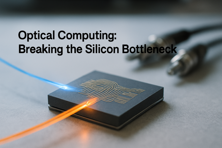
The relentless march of Moore’s Law is slowing. For decades, shrinking transistors on silicon wafers delivered exponential gains in computing power, but we are now bumping against fundamental physical limits. Electrons, the workhorses of modern electronics, generate heat as they race through ever-thinner wires, and leakage currents become harder to control at nanometer scales. Enter optical computing: a paradigm shift that replaces electrons with photons—particles of light—to perform calculations and move data. By leveraging the speed and bandwidth of light, optical computing promises to shatter the silicon bottleneck and unlock a new era of high-speed, energy-efficient processing.
Why Light Beats Electricity
Light has inherent advantages over electricity for computing. Photons travel at the speed of light in a vacuum (roughly 300,000 km/s) and can carry multiple signals simultaneously through wavelength-division multiplexing—the same technology that powers fiber-optic internet. In contrast, electrical signals in copper wires are slower, suffer from resistance and capacitance, and generate heat that limits clock speeds.
- Speed: Optical interconnects can transmit data at rates exceeding 100 Gbps per channel, while electrical interconnects top out around 25 Gbps.
- Bandwidth: A single optical fiber can carry hundreds of wavelengths, each acting as an independent channel, multiplying throughput without adding physical wires.
- Energy Efficiency: Photons do not generate resistive heat when traveling through transparent media. Early optical computing prototypes consume up to 80% less energy per bit compared to electronic equivalents.
These properties are especially critical for data centers, where power and cooling costs dominate operational expenses. According to a 2023 report by the International Energy Agency, data centers already account for about 1% of global electricity demand—a figure that could double by 2026 if efficiency gains don’t keep pace with AI workloads. Optical computing offers a direct path to reducing that footprint.
The Core Technologies Behind Optical Computing
Optical computing is not a single technology but a family of approaches that use light for logic, memory, or interconnects. The most mature area is optical interconnects—replacing copper wires with fiber optics or silicon photonic waveguides to move data between chips, racks, and even within a processor. Companies like Intel, IBM, and startups such as Lightmatter and Ayar Labs have demonstrated silicon photonic transceivers that integrate seamlessly with existing CMOS processes.
For actual computation—performing logic operations with light—researchers are exploring several methods:
- Photonic Integrated Circuits (PICs): These chips use waveguides, modulators, and detectors etched into silicon or indium phosphide to manipulate light. Mach-Zehnder interferometers can act as switches, while ring resonators enable wavelength-selective filtering.
- Optical Neural Networks: By encoding data into light beams and passing them through arrays of tunable beamsplitters, researchers can perform matrix multiplications at the speed of light—ideal for AI inference tasks. A 2022 paper in Nature Photonics reported a photonic neural network achieving 100 trillion operations per second (TOPS) while consuming under 1 watt.
- All-Optical Logic Gates: Using nonlinear optical effects (e.g., four-wave mixing or saturable absorption), scientists have built AND, OR, and NOT gates that operate without converting light to electricity. These remain largely experimental but promise the ultimate in speed.
Breaking the Silicon Bottleneck in Practice
The “silicon bottleneck” refers to three interrelated limits: thermal density (too much heat per square millimeter), interconnect bandwidth (wires can’t keep up), and transistor scaling (quantum tunneling and leakage). Optical computing addresses each directly.
- Thermal Density: Photonic circuits generate negligible heat in the signal path. Only the laser sources and photodetectors need power, and even those can be placed off-chip. This allows for denser packing of logic elements.
- Interconnect Bandwidth: Optical interconnects can carry terabytes of data per second across a chip or between servers. The US Department of Energy’s HPC program has already deployed optical links in supercomputers like Frontier to reduce data movement bottlenecks.
- Transistor Scaling: While photonic components are larger than individual transistors, they can perform complex functions (e.g., matrix multiplication) in a single step that would require thousands of electronic transistors. This shifts the trade-off from transistor count to photonic density.
A real-world example: In 2024, Lightmatter launched the Envise photonic accelerator, designed for AI inference. It claims to deliver 5x higher throughput per watt than leading GPU clusters, while reducing latency by an order of magnitude. Early customers include cloud providers testing it for large language model inference.
Challenges and Current Limitations
Despite its promise, optical computing is not a drop-in replacement for electronics. Several hurdles remain:
- On-Chip Light Sources: Integrating lasers directly onto silicon is difficult because silicon is an indirect bandgap semiconductor. Current solutions use external lasers or hybrid integration with III-V materials, adding cost and complexity.
- Optical Memory: Unlike electrons, photons do not interact strongly with each other, making it hard to store data in optical form. Most optical computing systems still convert light to electricity for memory access, creating a bottleneck.
- Manufacturing Precision: Photonic circuits require nanometer-scale alignment and low-loss waveguides. While silicon photonics leverages existing CMOS fabs, yields for complex circuits are still lower than for electronic chips.
- Temperature Sensitivity: The refractive index of silicon changes with temperature, causing phase shifts that can corrupt optical logic. Active thermal stabilization adds power overhead.
Nevertheless, the pace of progress is accelerating. A 2025 industry roadmap from the Photonic Integrated Circuit Consortium projects that photonic chips will reach commercial maturity for data center interconnects by 2028, and for general-purpose logic by 2035.
The Road Ahead: Hybrid Systems and Beyond
In the near term, the most practical deployments will be hybrid photonic-electronic systems. Here, light handles high-bandwidth data movement and specialized computations (like matrix multiplication), while conventional electronics manage control logic, memory, and general-purpose tasks. This approach minimizes risk while capturing the biggest gains.
Longer term, fully optical computers could emerge for specific workloads. For example, optical Fourier transforms are already used in lidar and signal processing. As manufacturing improves, we may see optical coprocessors for encryption, scientific simulations, and real-time video analysis.
The impact extends beyond raw speed. Optical computing could democratize access to high-performance computing by slashing energy costs, enabling edge devices to run sophisticated AI models locally. It could also unlock new applications in autonomous vehicles, 5G/6G networks, and real-time financial modeling—anywhere that latency and power are critical.
Conclusion
Optical computing is not a distant fantasy; it is a rapidly maturing field that is already breaking the silicon bottleneck in niche applications. By replacing electrons with photons, we gain speed, bandwidth, and efficiency that electronic systems can no longer deliver. The challenges of integration and manufacturing are real, but they are being solved one waveguide at a time.